![]()

Call us
+91-9880703082

Location
Bangalore, India and California, USA

Join Us
test
Current Openings
Physical Design Engineer (6+ Yrs) – 6 Positions (Onsite – Japan)
Tool experiences:
- ICC2, StarRC-XT (Layout)
- PrimeTime (STA)
Necessary skill & Experiences :
- Technology : 28nm technology experiences (Must)
: Less than 14nm technology experiences (Want) - Gate size : More than 10Mgates
- Hierarchical design : Hierarchy block and Top layout
- Power design : Multi power domain, Power management design (area power down, power switch, UPF)
- Program skill : Perl, Tcl etc.
Apply through linkedin
STA / SignOff Timing Closure
Experience: 3-5 Yrs (3 Positions)
- ASIC/SoC design & implementation experience with specific background in the areas of synthesis, SignOff STA
- Lower technology nodes like 40nm and below till 14nm/10nm.
Key Responsibilities:
- Includes definition and development of signoff methodology and corresponding implementation solution.
- Flow for STA, Crosstalk Delay and Crosstalk Noise analysis for digital ASIC/SoCs.
- Full chip timing constraints development, full chip / Sub-System STA and Signoff for a complex, multi-clock, multi-voltage SoC.
- Streamlining the timing signoff criterions, timing analysis methodologies and flows.
- Analyze and incorporate advance timing signoff flows (AOCV, POCV Based STA, IR Drop aware STA) into SoC timing signoff flow.
- Work for Systems and Architecture, SoC Integration, Verification, DFT, Mixed Signal, IP owners, Synthesis, Place & Route and other local/remote teams to address the design challenges in the context of the block, chip, and overall system.
- Concepts of CRPR, clock paths analysis and tweaks to meet timing.
- Multi Corner and MultiMode analysis.
- Close timing at SignOff corners covering the entire modes, delay corners for cells and interconnects.
Apply through linkedin
RTL Design
Job Location: Bangalore
Experience: 3 - 5 Yrs (2 Position)
Experience: 3 - 5 Yrs (2 Position)
Job Description:
RTL Design : Must have 3 to 15 years of practical experience with details of RTL development (VHDL and/or Verilog) including: functional and structural RTL design, design partitioning, simulation and regression, collaboration with design verification team. Must have good familiarity with latest RTL languages and tools, including: simulation systems (e.g. Modelsim, VCS), synthesis tools (e.g. Design Compile), static timing tools (e.g. Prime Time), Linting tools, CDC tools, UPF, code coverage, System Verilog Assertion, etc. Experience with the following area is highly desirable: Strong processor architecture knowledge Microarchitecture implementation Microprocessor integration Low power design Excellent verbal and written communication skills. Ability to work in a team environment. Good self-direction and time management skills.
Preferred Qualifications:
Develop RTL for multiple logic blocks of a DSP core Run various frontend tools to check for linting, clock domain crossing, synthesis, etc. Work with physical design team on design constrain and timing closure Work with power team on power optimization Work with verification team to collaborate on test plan, coverage plan, and coverage closure.
Education:
Bachelor's degree in Engineering, Information Systems, Computer Science, or related field.
Apply through linkedin
Physical Design Engineer
Job Location: Bangalore (10 Position)
Job Description:
Role & Responsibilities:
- Responsible for and own all aspects of physical design and physical verification effort at a block level.
- Worked on Netlist to GDSII at block level for multiple tape-outs.
- Expertise in hierarchical partitioning of block-level subsystems.
- Hands on experience in implementing high performance cores, low power designs.
- Flat timing closure of hierarchical sub systems with signoff STA.
- Block level floor planning, power planning and IR drop analysis.
- Formal verification at various levels of design hierarchy with respect to golden RTL.
- Debugging and solution finding skills.
- Liaising with Team members and co-workers and Design team for delivery of the project and in finding solution.
- Develop, support and maintain physical design flows and methodologies.
Desired Qualification:
- University degree (B.Tech/ M.Tech) in Electronics/ Electrical Engineering or similar. Other candidates will be considered if they have relevant experience.
- 3-7 Years of engineering experience primarily focussing on Physical design.
- Strong interpersonal skills, excellent verbal and written communication skills.
- Self-motivated and willing to take up additional responsibilities to contribute to the team’s success.
- Strong analytical, problem solving and debugging skills.
Desirable Experience:
- Experience in Power, Area with timing closure in parallel.
- Timing closure with Crosstalk and OCV (Advanced OCV), MMMC optimization.
- Working experience on various nodes viz. 65nm, 40nm, 28nm, 20nm, 14nm, 10nm.
- CTS and clock tree constraints creation for meeting clock specifications.
- Scan chain reordering / Scan Chain repartitioning.
- Timing ECO and Functional ECO implementation at Netlist stage.
- Good knowledge of standard cell libraries - circuit design and cell layout.
- Good understanding of STA, EM / IR and sign-off flows.
- High Performance Sub-Systems exposure.
- Understanding of Low Power Design (General Methodology, CPF, UPF).
- Physical Design Tool expertise viz. Cadence : Encounter / Innovus, Mentor Graphics: Olympus, Synopsys : ICC, ICC2, Atoptech : Aprisa.
- TCL / PERL Scripting and creating quick procedures for solutions will be a plus.
- Top level implementation will be an added advantage.
Apply through linkedin
STA Engineer
Lead role: 5 – 8 yrs range (3 position)
Job Description
Role & Responsibilities:
- Includes definition and development of signoff methodology and corresponding implementation solution.
- Flow for STA, Crosstalk Delay and Crosstalk Noise analysis for digital ASIC/SoCs.
- Full chip timing constraints development, full chip / Sub-System STA and Signoff for a complex, multi-clock, multi-voltage SoC.
- Streamlining the timing signoff criterions, timing analysis methodologies and flows.
- Analyze and incorporate advance timing signoff flows (AOCV, POCV Based STA, IR Drop aware STA) into SoC timing signoff flow.
- Work for Systems and Architecture, SoC Integration, Verification, DFT, Mixed Signal, IP owners, Synthesis, Place & Route and other local/remote teams to address the design challenges in the context of the block, chip, and overall system.
- Concepts of CRPR, clock paths analysis and tweaks to meet timing.
- Multi Corner and MultiMode analysis.
- Close timing at SignOff corners covering the entire modes, delay corners for cells and interconnects.
Desired Qualification:
- University degree (B.Tech/ M.Tech) in Electronics/ Electrical Engineering or similar. Other candidates will be considered if they have relevant experience.
- 3-7 Years of engineering experience primarily focussing on Physical design.
- Strong interpersonal skills, excellent verbal and written communication skills.
- Self-motivated and willing to take up additional responsibilities to contribute to the team’s success.
- Strong analytical, problem solving and debugging skills.
Desirable Experience:
- SoC/Chip level Timing closure and Signoff of high speed complex design with multiple clocks and power domains with minimal supervision.
- Working experience on lower technology nodes like 40nm and below till 14nm/10nm.
- Expertise in developing and owning Block and full chip Timing Constraints for complex, multi-clock, multi-voltage SoCs.
- Expertise in I/O constraints developments for Industry standard protocols would be an advantage.
- Good understanding of deep submicron parasitic effects, crosstalk effects, newer statistical timing approaches.
- Work with the Implementation team in having the SignOff Timing closure done.
Apply through linkedin
Embedded Requirements
(2 position)
JD1:
- Solid understanding of object-oriented design in C and C++, embedded platform.
- Knowledge of IBM Rational Rhapsody and development using UML.
- Knowledge of serial communication protocols, especially J1939, Hands on experience of CANalyzer.
- Experience using embedded debug tools such as JTAG/ICE debuggers, oscilloscopes.
- Familiarity with Git or ClearCase or any other version control tool in the agile software development process
JD2:
- 802.11 protocol testing experience.
- Excellent knowledge of IEEE 802.11 WLAN protocol and standards (802.11a, b, g, n, ac, d, h, I, k, r).
- Experience with wireless trace tools required (Omni peek, Wireshark).
- Experience configuring and managing network infrastructure and WLAN devices like Access Points and Switches required.
- Experience configuring and testing and troubleshooting networking technologies, WLAN security protocols (802.1x, AES/CCMP, etc.).
- Excellent problem solving ability with experience in diagnosing complex system issues including strong debugging skills.
- Ability to work in a fast paced environment and be a good team player.
- Bachelor’s degree from an accredited college or university in Computer Science, Computer Engineering or similar.
Apply through linkedin
Apply Now
About
BLR LABS PVT LTD
BLRLABS (Bangalore Labs) a technology pivot for co-designing hardware and software solutions. Our niche expertise enables us to offer services in Semiconductor Design and System Software at edge. We offer product engineering services for Internet of Things pan industry verticals, preferred partner from ideation stage to platform realization.
At BLRLABS (Bangalore Labs) we Co-create Next Generation products with our intellects, esteemed customers and technology partners. We take pride in being associated with academia, industry bodies and forums.
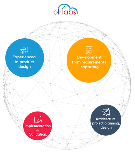
Our design services team works as extended engineering teams of product development companies to meet their product goals/schedules and help in mitigating challenges. With the flexible business models, BLRLABS (Bangalore Labs) extends services either in ODC mode or at client location to augment the customer engineering teams. The teams are experienced in product design and development from requirements capturing, architecture, project planning, design, implementation and validation.
At BLRLABS (Bangalore Labs) we Co-create Next Generation products with our intellects, esteemed customers and technology partners. We take pride in being associated with academia, industry bodies and forums.
Our design services team works as extended engineering teams of product development companies to meet their product goals/schedules and help in mitigating challenges. With the flexible business models, BLRLABS (Bangalore Labs) extends services either in ODC mode or at client location to augment the customer engineering teams. The teams are experienced in product design and development from requirements capturing, architecture, project planning, design, implementation and validation.
Meet our
BLR LABS PVT LTD
BLR LABS PVT LTD

RAVISHANKAR
BALASUBRAMANIAN
-CEO
BALASUBRAMANIAN
-CEO
Ravi is a serial entrepreneur and hands-on technology leader at BLRLABS. He posses 17 years of semiconductor industry experience with more than 50+ tapeout under his leadership. His updated skills in latest nodes still helps our leaders to drive our delivery on time. He hold a Masters degree from IISc,Bangalore. He is also known as a MasterChef of BLRLABS when it comes to cooking authentic Indian dishes.
Our Clients
.jpg)


.jpg)

All Rights Reserved By BLR LABS PVT LTD Sri Shanthi Towers | Privacy Policy 2018 | Site Map